
“the whole vid is worth watching”
Shows what QA looks like in a PCB factory
Full comment
In case anyone want to see how QA looks like in a factory, here's a video this video (the whole vid is worth watching)
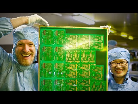
3.7M views · Jun 12, 2018 · 26:49 · 4 HN recommenders · 8 mentions · discussed 2018–2026
Strange Parts tours JLCPCB's large PCB factory in Huizhou, China, walking through the printed circuit board manufacturing process step by step. It shows the machinery, quality checks and scale behind cheap prototype boards.
Why Hacker News points people here: Recommended as the best look inside a modern PCB fab, cited in threads on hobby PCB vendors, manufacturing in China and automation.
“It's a tour of JLCPCB's factory, where they go through all the PCB manufacturing steps.”HN comment, 2023
“the whole vid is worth watching”
Shows what QA looks like in a PCB factory
In case anyone want to see how QA looks like in a factory, here's a video this video (the whole vid is worth watching)
“Strange Parts[1] made a great factory tour video of the JLC facility in China”
Factory tour of JLC's PCB facility in China.
Strange Parts[1] made a great factory tour video of the JLC facility in China for anyone that interested in such things: this video [1] link
“Strange parts has some cool inside look at the popular pcb manufacturing fabs”
Inside look at PCB fabs like PCBWay and JLCPCB.
Strange parts has some cool inside look at the popular pcb manufacturing fabs such as pcbway and jlcpcb this video
“It's a tour of JLCPCB's factory, where they go through all the PCB manufacturing steps.”
Tour of JLCPCB's factory covering all PCB manufacturing steps.
This is very interesting: this video It's a tour of JLCPCB's factory, where they go through all the PCB manufacturing steps. (They just cover the PBC itself, not the assembly service.)
“Here's a step-by-step video about how JLCPCB makes PCB's.”
Step-by-step view of JLCPCB board cutting with CNC router and vacuum table.
Here's a step-by-step video about how JLCPCB makes PCB's. The link goes directly to that step at 21:09: this video It looks like in this case they are using a CNC router to make the cuts, and a vacuum table to keep the PCB's in place (it's a table with a grid of tiny holes that has vacuum inside to suck the PCB's onto the table).
“You might as well watch the entire process of how JLCPCB works”
Shows the full JLCPCB process, cited to dispute easy automation.
You might as well watch the entire process of how JLCPCB works and then tell me if all of that can be "automated": this video
Cited for engineers doing customer support enabling cheap hobbyist PCBs.
Who in Japan is good at this? I can only imagine the R&D division at maybe Playstation and thats it. China has so many people that EE and CS are a dime a dozen, thats why they have a competitive market thats low cost. People are in a jungle trying to survive. [0]: this video The video is (Supposedly) EEs doing customer support roles thus allowing Cheap PCB for hobbyists, the equivalent in the US does not exist. Side Note: I hear this is also why SASS never really took off in China. Why pay someone else for software when you can get a dozen people to make your own cheaper.
Cited as example of free engineer review in cheap PCB service.
Yeah I didn't say that Chinese people didn't want to go down the same route, infact lifestyle influencers have a better shot there (probably 0.1% better). There is so much overproduction of engineers that you are possibly working a customer support role with that degree. Another reason SASS supposedly never took off there, why pay some company when you can just hire from the batch of overproduced STEM graduates and make any software you need. When I can have an experienced engineer correct my garbage designs for free as part of a manufacturing service you know I am benefiting off of a lucky circumstance that will go away one day: this video