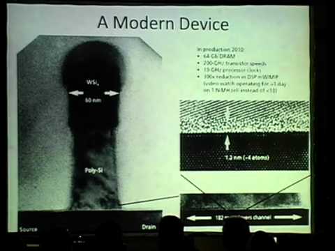
A HOPE09 talk on how modern computer chips are manufactured, from 22nm transistors to ultra-clean fabs and the tricks used to pattern tiny features with light. It frames chipmaking as hacking electrical engineering and physics.
Why Hacker News points people here: HN repeatedly calls it the best in-depth introduction to IC manufacturing, a sense-of-awe talk by an independent engineer, while wishing for an updated version.
“This talk on YouTube is the most in depth explanation of IC manufacuring I have seen. I highly recommend it to anyone, no matter their background.”HN comment, 2018
“I very much recommend everyone to watch this video, to get a sense for the complexity that goes into producing a modern CPU.”
Shows the complexity of producing a modern CPU, with a chip cross-section.
Full comment
There's a brilliant talk, given in 2009 at HOPE09, NYC titled "Indistinguishable From Magic: Manufacturing Modern Computer Chips". At roughly 36 minutes, there's a cross-section of a (in 2009) modern chip. The topmost layer is the shiny rainbowy topmost metal-layer you see on typical (from the top) die photographs. The very, very small comb-looking bottommost-layer is the individual transistors, and structures there are of the size that give a "xxx nm" process its name. this video I very much recommend everyone to watch this video, to get a sense for the complexity that goes into producing a modern CPU. To come back to the thread I'm answering here: The logic analyzer on the Alto (probing microcode) connected to interconnects of individual gates probably would be connected to signals somewhere in the lower middle of the stack in a modern CPU, I guess.
Strongly recommendsahakkiJun 2018
“This talk on YouTube is the most in depth explanation of IC manufacuring I have seen. I highly recommend it to anyone, no matter their background.”
In-depth explanation of IC manufacturing, still mostly applicable despite age
Full comment
this video This talk on YouTube is the most in depth explanation of IC manufacuring I have seen. I highly recommend it to anyone, no matter their background. You really gain an appreciation of how insanely complex modern computers are. It’s from 2012 but he talks extensivly about how (2012-)future chips will be made. And most of the information is still applicable.
Strongly recommendsmanigandhamAug 2018
“it's one of the best videos available on how chips are actually built and gives a great overview”
Great overview of how chips are actually built
Full comment
I highly recommend watching this, it's one of the best videos available on how chips are actually built and gives a great overview: "Indistinguishable From Magic: Manufacturing Modern Computer Chips" - this video
Strongly recommendsQub3dOct 2018
“This talk is delivered really well and always leaves me with a sense of awe in how CRAZY it is that humans figured out integrated circuits.”
Well-delivered talk on integrated circuits, explains Intel's process node difficulties
Full comment
Indistinguishable From Magic: Manufacturing Modern Computer Chips [0]. This talk is delivered really well and always leaves me with a sense of awe in how CRAZY it is that humans figured out integrated circuits. Its a bit out of date, but it gives enough of a peek under the hood to understand why Intel has had such difficulties going to 10 and 7mn processes[1]. [0]: this video [1]: link
Strongly recommendssl-1Dec 2019
“Best resource I have run in to about this is this talk”
Introduces the hacks used to get tiny features on silicon
Full comment
Best resource I have run in to about this is this talk: this video It quickly introduces the various hacks we do in order to get ~30nm features on silicon. But the talk is quite dated (early 2010's), but never ceases to amaze me. Semiconductors are indistinguishable from magic indeed.
Strongly recommendsolliejMar 2020
“My favourite video on them is this one from many years ago, it’s a presentation by an engineer not being paid by a fab”
Independent engineer presentation on fabs, better than corporate ad video
Full comment
I found this to be basically an ad. My favourite video on them is this one from many years ago, it’s a presentation by an engineer not being paid by a fab: this video
Strongly recommendsTrainedMonkeyApr 2020
“but entire video is amazing”
Entire talk is amazing for those who find the topic cool
Full comment
If you think this is cool, watch this video. I've linked a relevant to the comment portion, but entire video is amazing: this video P.S. if anyone knows a more modern version of this talk, I would love to see it.
Strongly recommendsgary_0Jul 2024
“If you haven't watched this video, I highly recommend it”
Comprehensive look at how nuts the chip business is
Full comment
It takes years just to figure out how to use the machines to produce actual working chips. They're the most specialized, intricate, expensive machines in the world. They're operated in enormous clean rooms that only allow for 1 half-micron sized particle per cubic foot. No fab is going to run them without exactly following the procedures they have spent billions developing and testing. They are also going to avoid potential delays as much as possible because these machines have to be running for as much of their useful life as possible to recoup the vast expense. The level of risk-averseness is insane, but warranted. If you haven't watched this video, I highly recommend it: Indistinguishable From Magic: Manufacturing Modern Computer Chips this video It's a little outdated now, but very comprehensive and gives you an idea of how totally nuts the chip business is.
RecommendstcasApr 2016
“this video which goes over a lot of modern chip fabrication techniques, circa 2009”
Overview of modern chip fabrication techniques circa 2009.
Full comment
I do not have the answers for your questions (and I don't think anyone can share actual failure rates), but I would direct you this video which goes over a lot of modern chip fabrication techniques, circa 2009: this video It's crazy stuff. There are wafer test machines which will interface with the wafer directly and do some testing (which are $$$$), JTAG type tests, which access parts of the chip out of band, and functional testing. Some products, like SD Cards actually have a microcontroller on board that will provide the test routines and error correction without the need of an expensive machine. Design for test is extremely important. I'm by no means an expert however, I mostly deal with JTAG and functional tests.
Recommendsavs733May 2016
“I did a talk on the scale and economics and so forth a while back you might find interesting”
Talk on scale and economics of chip manufacturing.
Full comment
If you forgive the shameless self-promotion, I did a talk on the scale and economics and so forth a while back you might find interesting: this video It has been posted on HN a few times before...the technology still puts a tingle in my spine [insert critcism of how I need to be a better public speaker here]
RecommendsjacquesmApr 2017
“There was a fantastic video about IC manufacturing linked here on HN a while ago”
Video about IC manufacturing.
Full comment
There are some exotic processes that give better performance but the economies of scale aren't there yet and the cost of production is probably always going to be much higher than that of Silicon, which is after all a very abundant element on Earth. There was a fantastic video about IC manufacturing linked here on HN a while ago, I'm not sure if I'll be able to find it. edit: Hah, found it :) this video
RecommendstaspeotisJan 2018
“Recently I saw this video [1] and only juuust started to get an inkling as to how big the problem space is.”
Conveys the huge complexity of modern CPU manufacturing
Full comment
I can't even begin to comprehend the complexity in a contemporary CPU. Recently I saw this video [1] and only juuust started to get an inkling as to how big the problem space is. [1] this video
RecommendssaganusMar 2020
“Just amazing. I wish a newer video explaining more recent technologies was available.”
Amazing look at modern chip manufacturing, though dated
Full comment
Sounds like this video: Indistinguishable from magic: Manufacturing modern computer chips this video Just amazing. I wish a newer video explaining more recent technologies was available.
RecommendsSonOfLilitJul 2020
“This is a great talk on the history of chip processes”
Great talk on history of chip processes
Full comment
Each additional step requires solving a lot of new engineering problems and usually some new physics too, and it's not a linear process: many techniques are proposed that become cost effective only when previous techniques hit their size limits, and then a lot of research is done and most techniques are never gotten to work at scale and just a few pan out and become the next process. This is a great talk on the history of chip processes: this video This is about some of the challenges that had to be solved for a current modern process: link
RecommendsxoaSep 2020
“I was blown away already watching the "Indistinguishable From Magic: Manufacturing Modern Computer Chips" [2] presentation years ago”
Incredible presentation on chip manufacturing, though about old tech
Full comment
Just doing some napkin math to give myself some other context in my own head with something much smaller, die size for the Apple A14 isn't out yet, but the A13 (found in the iPhone 11 series and SE 2) is around 98mm^2 manufactured on TSMC's 2nd gen 7nm N7P. A14 might be something like that, because while it's a smaller process Apple boosted transistor count by 38% as well. Lazily/conservatively taking off 10mm on the edge for squares into a circle, that'd be about 630 chips per N5 wafer, a high enough count that chip loss rate shouldn't be too far from defect rate. Even assuming they can get 90% yield right out the gate (maybe generous) that's still about $30/chip, just for manufacturing without any R&D amortization, packaging etc. That actually seems not insignificant going by historical iPhone BOMs [1], so even for smartphones with their far far smaller SoCs 5nm at launch isn't nothing. The continued ongoing progress in silicon is just mindblowing when you dig into the details in any real way. I was blown away already watching the "Indistinguishable From Magic: Manufacturing Modern Computer Chips" [2] presentation years ago, which still seems incredible and yet that's all talking about now ancient tech. The increasing costs and design challenges though are also going to have interesting effects on the industry, as who/what has the margins to afford fabbing aggressive chips on the cutting edge might start to diverge a bit more. I also wonder how longevity will be, I remember
Recommendsta988Jun 2021
“It is getting "old" but this great video is covering it”
Covers mask simulation and chip making, somewhat old
Full comment
Yes that's pretty similar to what is used. Each mask takes days to get simulated. It is getting "old" but this great video is covering it this video
RecommendsjoshAgAug 2021
“does a great job putting this machine into perspective in teh chip making process”
Puts lithography machine in perspective of chip making, though a decade old
Full comment
This video is in the same vein, and does a great job putting this machine into perspective in teh chip making process, but it's sadly a decade old now. this video
RecommendsalyandonJul 2022
“I would love to see an updated version of this video”
Magical-seeming chip making; commenter wants an updated version
Full comment
Magic (at least as far as I'm concerned). I would love to see an updated version of this video: this video
RecommendscalebmDec 2022
“shows just how magical they are”
Shows how magical silicon chip manufacturing is
Full comment
This talk on how silicon chips are manufactured, called "Indistinguishable from Magic" shows just how magical they are: this video
Cites itbaneAug 2017
“From that point the process was basically what's in the rest of this video”
Shows rest of chip lithography process, compared to offset printing
Full comment
This is strikingly similar to the process used in modern offset printing. As a young child, I grew up in a family printing business, and though I didn't learn all the details (I didn't really have much interest in the printing side of the business and spent most of my time in the then still very early digital prepress playing with the computers). My earliest memories of it were marked by specialists doing digital typography on specialist computers, one monitor was a green-screen where some kind of markup was entered and the other screen was a raster monitor where the output was rendered. Each block of text was "printed" on photographic paper, cut and then sent to the "layout" department where it was taped or wax adhered to a page. (If this is hard to picture, imagine taping each block of text from this page [1] onto another piece of paper in order to layout the entire page.) The process looked a bit like this [2] Then the final page was photographed in a photography room and the negative developed. On occasion a photographic "proof" would be developed to show the final page layout and make sure there weren't any artifacts from all these tiny little pieces of paper that were used to make up the text blocks. Then the negative was used as a lithographic mask to "burn" the image of the page onto a metal sheet which then went through some kind of chemical bath to etch the image onto the sheet. From that point the process was basically what's in the rest of this video [3]. And one